As part of my course’s labs, we had to design a RFID reader board. This project served two purposes; it let us use the skills learned in our communications system lectures, and also gain practical experience in PCB design. This project was done in partnership with Harry Beadle.
The board is designed to operate with 125kHz tags. These have been superseded by 13 MHz ISM tags for most modern applications. 125kHz is still the standard for animal chipping though. (I haven’t found a test subject to confirm this yet!)
The project started out with an introduction to circuit simulation. An analogue filter and demodulator was designed in NI’s MultiSim. It was very satisfying to see the behaviour we’d been shown mathematically come to life, and a demodulator spring to life from individual blocks.
CAD Design
Next Eagle was used, and footprints were created for an LCD display and a buzzer. The LCD footprint was certainly a challenge, as the datasheet was fairly tricky to read. Fortunately it worked out ok.
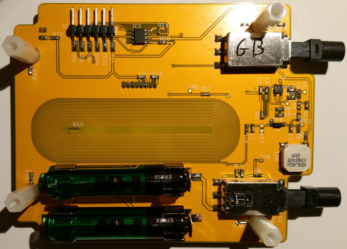
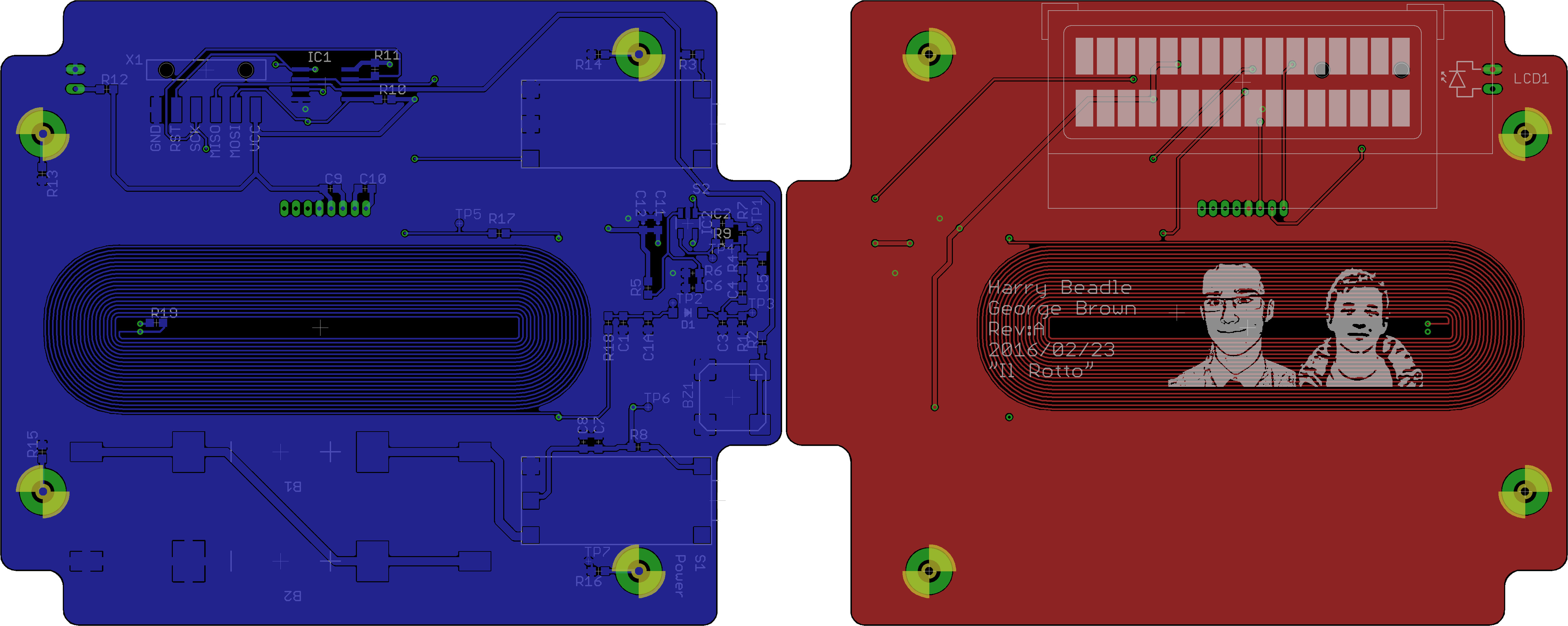
The schematic was captured in eagle from a partially provided design. Changes where then made to add test points, and add a few extra features, like optional grounded mounting holes.
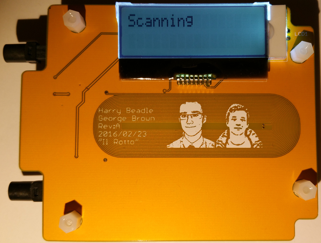
The PCB was then placed and layed out. The board outline and and hole spacing was provided to fit an enclosure. Unfortunately, we weren’t shown the enclosure, so our display ended up just at the boundary of the frosted part of the case.
To personalise the board, Harry processed some photographs in Photoshop to generate black and white graphics, and large enough features to render properly in silkscreen. The resulting bitmaps are imported into the TopSilk layer in Eagle with a ULP that is shipped with the program. I was particularly satisfied by how these came out on the finished board.
This was the finished layout that went for manufacture:
Assembly
The circuit mount assembly was done by hand in the space of about 3 hours. For my first major SMD board I was very pleased with how the soldering came out!
The assembly proved to get much easier in this time. Just a small amount of experience makes a big difference to the ease of SMD soldering. I know now that assembling the circuit should probably be done from the inside of the board. I found it was sometimes tricky to get the iron into devices that were surrounded by other components. Next time I’d also make an effort to set out a sheet of labelled components. I found a fair amount of time was checking component values before fitting them to the board.
Testing and Evaluation
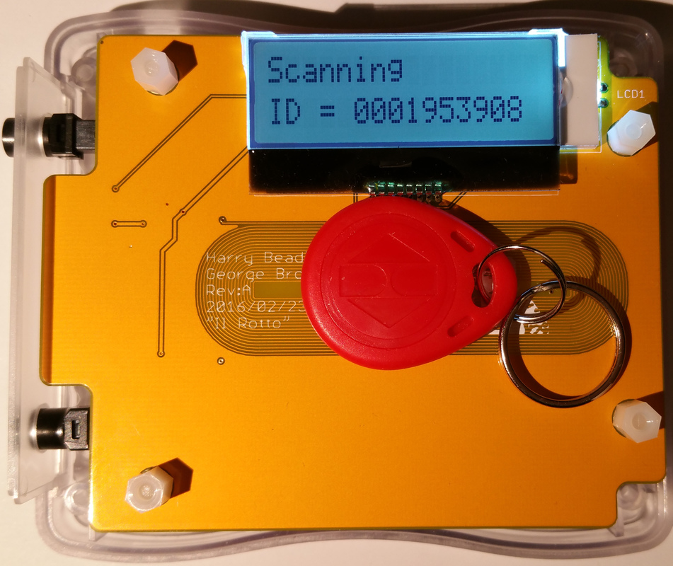
Somewhat amazingly, once programmed, the board worked perfectly first try! The antenna is not ideal, and we didn’t have sufficient time during the lab to tune the coil properly. As a result, the tag is only read when within about 5 mm of the PCB, but I’m sure this could be improved with some time tuning the coil.
From the two AAA cells, the device draws 50 mA. Much of this is used in lighting the LEDs and backlight.
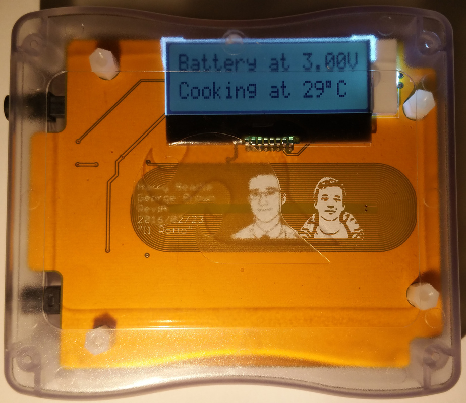
Finished Prototype