During my A-Levels my chemistry teacher started up an element collection. As a leaving gift, I felt it would be good to provide a sample of perhaps the most important element in electronics to the collection.
Decapping ICs to extract their silicon goodies inside is an often discussed topic on electronics forums. The epoxy of a standard DIP package is remarkably strong and resistant stuff. An often documented method is to heat the device in a puddle of nitric acid. Ben Krasnow documented his version of the process here. Unfortunately, at the time of writing I don’t have a hot plate, or concentrated nitric acid. Being time sensitive I decided it was best to push on with other options, rather than wait for postage!
My first thought was that the epoxy may be sufficiently brittle to come away with a good smack from a hammer. This method initially produced promising results, with the epoxy cracking open. I was fearful though that the die would be damaged by repeated blows. At this point I recalled a method I’d heard of involving use of a blowtorch to destroy the epoxy. Unfortunately, I cannot recall the source of this idea. It may have been an instructable, or a Picaxe forum post, but I can no longer find it.
Attempt 1
First, venture to the garden, arrange a stack of bricks into a BBQ of IC death. Fetch a blowtorch, some dead ICs, and some pliers. For these trials I used 14 pin DIPs.
My first attempt was to simply blast the device with heat while rotating it in the flame with pliers. Eventually the epoxy started to crumble away. With the melting point of silicon being 1414°C, I was confident my blowtorch wouldn’t get things hot enough to melt the die itself. Unfortunately I was wrong.
I’d spent maybe a couple of minutes blasting it, at which point the leadframe melted a bit and the whole device glowed red hot. After leaving the package to cool I crumbled away what was left of the epoxy to find a unassuming silver sphere. Oh well, try again…
Attempt 2
For my second attempt I tried heating the device in bursts until the epoxy crumbled away. Unfortunately it seems this approach has a similar effect on the die!
It appears all of the other elements in the dies significantly reduce the melting point.
Attempt 3
It was clear very little heat was actually needed. For my final attempt I bent the leads flat so the bottom of the chip was flat against the brick. This way we’re only transferring heat to the top of the IC, rather than the whole thing.
Next I heated the device about 3 times with 5 second bursts. (Cooking times vary by device size, I’m using 14 pin DIPs.)
The plastic will turn white in places, and will feel brittle. (Let it cool before you touch it!) At this point I whack the case with the pliers until most of the plastic comes away. Be careful not to ping the die off across the garden!
Results
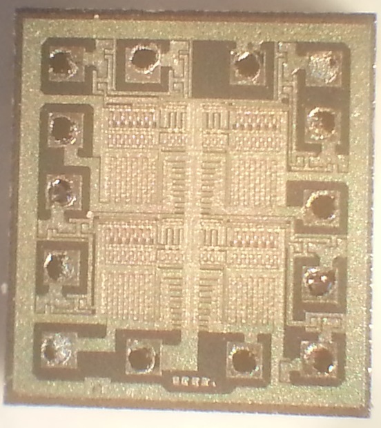
With the technique sorted, I repeated the process on two other chips, all of which were dead before hand. I freed a PIC16F84A, a HCF4511, and a 74HC00. These all yielded fairly small dies. I popped them under the microscope and captured a few pictures.
First, the PIC, which has a 2x3mm; die, and features sufficiently small to get diffraction colours:

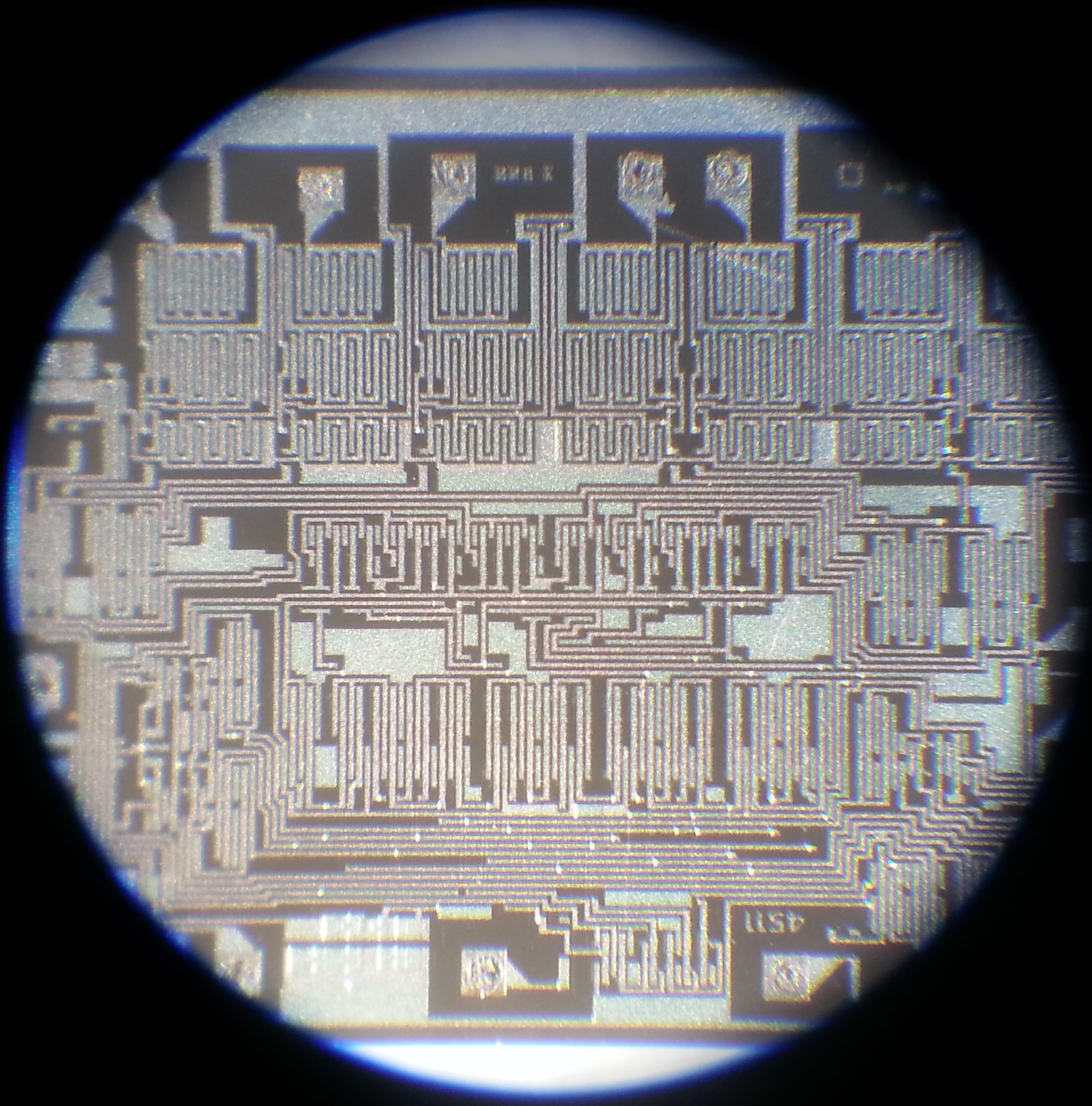
Next, the 4511, which is designed to deliver more power, so has a larger feature size. This die is 3x1.5mm;
Finally, the very simple 7400. Here you can clearly see the four distinct gates.
Evaluation
Overall I was fairly pleased for a project that only took a little time to do. If I have a chance again in the future I’d like to refine the method further.
Of course, the approach is fairly brutal. The HNO3 method leaves a device essentially in-tact, and as Ben showed, the device can survive the ordeal. My approach totally destroys the bond wires, and probably the dies too!
I’d also like to try a larger device so we can see more detail. Perhaps SMD packages could be tried too. They could potentially be easier to get into.